
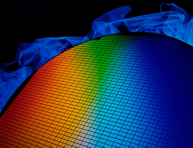
The wafer is defined as a crystalline substrate used to integrate electronic components. These semiconductors are used for building an integrated circuit through different processes like etching, implantation and doping.
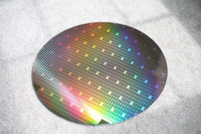
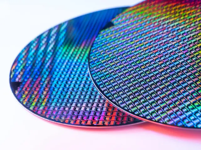
Due to the umpteenth benefits of patterned wafers over regular unpatterned wafers, the demand for this material has increased exponentially in the semiconductor industry recently. Patterned wafers possess similar cleaning requirements and quality as compared to regular wafers; however, they possess better uniformity and therefore are considered as more reliable in usage.
Here is a detailed guide explaining the step-to-step process of manufacturing patterned wafers, the evolution of these semiconductor materials over the years, and their various applications. Stick to the end of the article to understand the important factors to consider while purchasing patterned wafers.
History Of Patterned Wafers
In the 1950-60s, chip technology used basic integration technologies with few resistors and transistors; as the manufacturing process advanced, the demand for advanced semiconductors increased. Using photolithography which involved coating patterns on a wafer, the possibility of creating sophisticated chips proved to be a significant step. Precise and minute patterns could be manufactured for the devices after that.
Manufacturing Of Patterned Wafers
The process of making patterned wafers is known as photolithography and involves a variety of steps.
- It involves the separation of the etched puddles. An ion beam is used in the making process, which can form a large puddle. Therefore, manufacturers use larger wafers and increase the chips per puddle.
- Determination of crystallographic puddles is essential in the manufacture of patterned wafers. Bulk micromachining and microstructures do not require primary flat misalignment. The accurate determination of the crystallographic direction is essential for the manufacture.
- An X-ray diffraction method is used to avoid undercutting of the patterned puddles at the edges.
- Using a chemical etching solution, the puddle gets etched by removing the crystalline layer. This results in the formation of a patterned sludge.
- Layers get stacked in the formation of the patterned puddle. An atom with a single hydrogen atom forms a patterned puddle.
- When the etched puddle gets patterned by the phosphorus puddle, it results in 111 planes. Thin patterned puddles are used to develop advanced MOS devices, and thick epitaxial puddles are used towards consumption and energy efficiency.
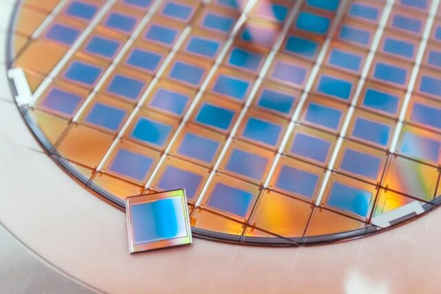
- The formed microelectronic device is cut using a wire saw, resulting in the formation of the wafer.
Applications Of Patterned Wafers
Patterned wafers have been extensively used in important sectors like health, energy and electronics.
The electronic industry creates semiconductor devices, and integrated circuits align with the demands of smaller, more potent and quick gadgets. On the other hand, in the medical industry, patterned wafers are used in microfluidics. These materials can be used extensively in the construction of drug deliverance systems, diagnostics and other medical-related applications.
The use of these semiconductor materials has been exponentially increased in the manufacture of photovoltaic cells to make the construction of solar panels easy, affordable and more efficient as well. The patterning wafers will help in increasing the effectiveness of trapping solar energy.
The optic industry has also used patterning wafers in various optical components, including filters, diffraction gratings and lenses. These patterned wafers can be designed to affluence the light differently.
With the advancement of technology, these patterning materials have been used for more detailed patterns increasing the productivity of semiconductor devices. It has now been used to decorate and calibrate the chip manufacturing equipment.
What The Future Holds?
The process of manufacturing patterned wafers is expensive and time-consuming. However, the future holds vast possibilities for patterned wafers. As it has already been quite clear, these semiconductor devices have established themselves as the hallmark of advancing technology.
These materials are one of the most crucial components of smartphones, laptops, and other electronic devices and have shown increasing ineffectiveness in other related fields, especially optics. Professionals suggest that the demand for sophisticated sensors and microprocessors will further increase the advancement of these chips.
What Should You Consider?
The development of sophisticated patterning semiconductor devices has been increasingly reducing defect tolerance. As the manufacturing stems into nano levels, inspecting the wafers is becoming more than ever. Methods like differential image detection, DUV wafer inspection, E-beam water inspection, motion control and custom optical solutions are used for inspecting the patterned wafers.
The popular materials generally used for wafer production are Silicon, GaAs, Germanium, Sapphire and InP (Indium and Phosphorus). In most scenarios, silicon is the most commonly used as it is easiest to extract compared to other semiconductor materials and therefore is an affordable option.
On the other hand, the usage of GaAs, Germanium, Sapphire or InP has exponentially increased as well due to the various potent benefits it provides to the manufacturers. Due to the possession of high electron mobility, GaAs provide effective resistance to heat. Sapphire and InP also provide high electron velocity and have been effectively creating a stronghold in the industry; using these materials can prove to be expensive.
While purchasing patterned wafers, consider factors like budget, grade of the substrate used, and quality of wafer being sold after meeting specifications like particle density, flatness, cracks or saucer pits. It is essential to purchase patterned wafers from reputable sources. You can search for good manufacturers of these semiconductor materials according to your location, review the customer reviews and decide accordingly.
Bottom Line
Patterned wafers are considered the bases of electronic devices; the patterned wafers might vary in a few characteristics and be quite expensive compared to regular unpatterned wafers. However, professionals guarantee that the use of patterned wafers will increase in the coming years due to their increased resistance to heat and durability. Patterned wafers have an increased shelf-life proving to be cost-effective and advantageous in the long run.
Now with the detailed knowledge of the manufacturing process, the various applications of patterned wafers and various prospects of its usage in the future; you can now make an informed decision while purchasing the materials. Always consider purchasing patterned wafers from a reputable source. It is also essential to place the semiconductor device on various detection tests before making your final decision.


